Semiconductor metrology
How to improve the wafer production process and ensure high-quality wafers
To support you in producing the highest-quality wafers, Anton Paar provides wafer metrology tools for monitoring the quality of your thin films, understanding the surface chemistry of outer layers, and characterizing wafer defects. Our instruments will help you determine and adjust many different parameters throughout the wafer manufacturing process to create a better end product.
Wafer metrology in the production process
From thin films to testing, assembly, and packaging, our measurement solutions support you at every manufacturing step.
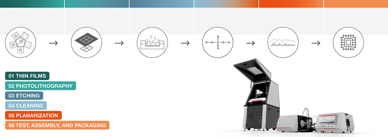
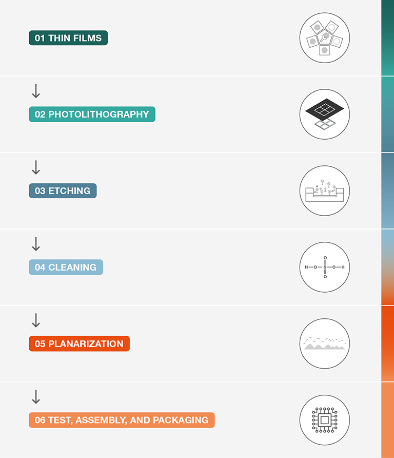
Thin films
It is important to have full control over the parameters influencing the thin film deposition process and measuring instruments which monitor these parameters can support you here. As thin films usually have a thickness between a few nanometers and about 100 micrometers, and in some cases even a few atoms, this requires wafer metrology instruments that operate in the nano- and sub-nanometer range. To analyze the proper adhesion, scratch resistance, and hardness of the layers and therefore ensure the quality of the end product and further production steps, you need to apply scratch testing and instrumented indentation testing. These methods give insight into the mechanical properties of the deposited layers.
Measuring the zeta potential of the outer layer with Anton Paar’s surface charge analyzer provides you with information on its surface chemistry and thus its composition.
The structural features of thin films can also be investigated by GISAXS (grazing-incidence small-angle x-ray scattering) using the Anton Paar SAXSpoint 5.0 system. Due to the nature of X-rays, this method not only probes structures on the surface but also gives information on features “buried” below the surface.
Photolithography
To help avoid contamination of the photomasks after the cleaning process, you can perform a zeta potential analysis and use the results to optimize the cleaning process.
Etching
To achieve reproducible etching results you need to be in full control of the concentration of the hydrofluoric acid used. Anton Paar’s density meter with a chemically resistant measuring cell delivers concentration values in minutes so you can obtain consistent etching.
Different etching strategies also have an effect on the surface chemistry of the wafer. Make use of zeta potential analysis with Anton Paar’s surface charge analyzer to follow the effect of etching on the outermost wafer surface.
Cleaning
Cleaning is a critical step in the manufacturing process of wafers, requiring the removal of chemical and particle impurities without altering or damaging the wafer surface or substrate. Anton Paar’s measuring devices help you keep the following under control:
Sulfuric acid concentration
One of the most important parameters is the concentration of the sulfuric acid which you can measure with a chemically resistant density and sound velocity meter or with a process sensor. Exact knowledge of the concentration of the sulfuric acid guarantees a consistent cleaning process.
Purity of ultrapure water
Properly functioning membranes are a prerequisite to having ultrapure water for the cleaning process. Using a surface charge analyzer to determine the zeta potential of the membrane-water interface gives you a clear understanding of the membrane’s behavior. Unexpected membrane fouling can thus be prevented and you can step in before there is degradation of the water purity.
To speed up and improve the cleaning process, you can use a refractometer to check the purity of the cleaning agent to ensure proper cleaning without residues on the surface.
Browse solutions
Planarization
To support you during planarization, Anton Paar provides two devices for reducing contamination in these process steps: one for solids, one for particles. Evaluating polishing pads and slurry particles by determining the zeta potential gives you the knowledge you need to decide when to replace pads based on their performance. Zeta potential measurements on wafer surfaces and slurry particles used in the CMP process alert you to the potential for particle adhesion due to electrostatic interactions. With this knowledge you can optimize the conditions to prevent this from happening.
The open and closed porosity of pads is quickly quantified by gas pycnometry which allows producers to monitor quality and aids users in selecting the optimal pad for their process and the particular slurry used.
Continuous inline monitoring of slurry properties in CMP during planarization provides real-time data to help you control the slurry’s health and detect changes in abrasive concentration. A stable slurry density within the specification limits guarantees the production of a high-quality wafer surface.
Testing, assembly, and packaging
The right packaging is essential to save the precious wafers from damage. Therefore it is important to ensure that the used materials (bond pads, connections, and ball grid arrays) have the correct mechanical properties. You can face this challenge by performing measurements on predefined spots on the microchip to determine the hardness and elastic modulus with a nanoindentation tester and/or ultra nanoindentation tester.
Further related applications
Measuring the particle size distribution of the crystalline silicon as well as monitoring the amount of fine and cohesive particles (<10 µm) ensures the final purity grade provided by well-established processes including grinding (size reduction) and chemical treatment steps.
The determination of inorganic impurities is important to ensure the quality of base materials and the correct functionality of final products. With microwave-assisted sample preparation from Anton Paar you can count on reliable digestion results for every sample type.
Surface characterization is also an important task for products related to wafer production such as displays and optoelectronics. When manufacturing displays you can measure the adhesion with a micro scratch or nano scratch tester and evaluate the mechanical properties with a nanoindentation tester or a combination of both methods. The results will give you insights into and full control of the layer quality.
Find your solution
| Solution | Your benefit | Instrument | |
| Thin films | |||
| You want to monitor the quality of thin-film coatings. | Perform surface charge analysis (zeta potential measurements) at the outermost surface layer. Use GISAXS to characterize structures on or below your surface. | Information on the surface chemistry that confirms the desired composition of the outermost thin film layer; information about the coating quality and nanostructure distribution of your thin film | |
| As an integrated circuit (IC) designer and manufacturer, you want to ensure that the materials and layers used in IC production have the correct mechanical properties. | Characterize the hardness and elastic modulus and adhesion of thin layers on wafers with mechanical surface characterization (using nano scratch testing and low-load indentation testing). | Full control of the deposited functional layers during the integrated circuit development | |
| Photolithography | |||
| You want to avoid contamination of photomasks, which affects the quality of integrated circuits. | Determine the correlation between different cleaning agents and the photomask by measuring the zeta potential ( surface charge analysis). | Optimization of the performance of cleaning procedures for photomasks | |
| Etching | |||
| You want to determine the concentration of the hydrofluoric acid to get a consistent etching performance. | Perform a concentration measurement with a chemically resistant Hastelloy U-tube density meter to determine the hydrofluoric acid concentration. | Reproducible etching processes by quickly checking the acid concentration beforehand | |
| Cleaning | |||
| You want to quickly determine the concentration of sulfuric acid, approx. ten times faster than with the traditional titration method. | Measure density and sound velocity with one instrument ( concentration measurement). Due to the non-linear concentration curve of sulfuric acid both technologies are required. | High repeatability and reproducibility of the cleaning process |
|
| You want high-performance process concentration measurement of sulfuric acid. | Perform concentration measurement wherever H2SO4 determination is required and cover the entire concentration range of H2SO4 (0 % to 100 %). | Continuous quality monitoring of your cleaning process | |
| You want to ensure proper cleaning without residues on the surface. | Perform a purity measurement of the cleaning agent (e.g. ultrapure water) with a highly precise refractometer. | Acceleration and improvement of cleaning process to save time and resources | |
| You need to ensure the membrane quality to get ultrapure water for semiconductor processes. | Determine the membrane’s surface zeta potential ( surface charge analysis) to monitor the membrane quality and prevent unexpected membrane fouling and the degrading of water purity. | Reliable water purity for semiconductor device manufacturing | |
| You want to ensure that your CMP slurry delivers consistent results during polishing. | Measure the viscosity of your CMP slurry to gain information about its flow behavior and performance during the CMP process. | Ensuring reproducible polishing performance and thus consistent wafer quality. | |
| Planarization | |||
| You want to avoid contamination of silicon wafers with different top coatings due to contact with components of the slurry during the process of CMP. | Determine the zeta potential of wafer surfaces and slurry particles with surface charge analysis to optimize process conditions and avoid particle adhesion through electrostatic interactions. | Reduced cycle times in post-CMP cleaning thus increasing throughput | |
| It is important for you to avoid cross-contamination in CMP processes through polishing pads. | Characterize polishing pads and slurry particles with surface charge analysis to predict electrostatic attraction. | Reduction of the replacement frequency of polishing pads to save time and money | |
| You want to guarantee the correct particle size distribution in your slurry. | Characterize the slurry particle size with particle size analysis. | Improvement of polishing performance to reduce damages to the wafer surface | |
| You need to ensure consistent microstructure from pad lot to lot. | Determine open and closed porosity with solid density measurements done by gas pycnometry. | Assured pad selection and continuity of process parameters | |
| You want to inline-monitor your slurry properties in the CMP process. | Perform slurry density measurement with a process density sensor. | Inline monitoring provides real-time data to indicate slurry health and to detect changes in abrasive concentration. | |
| Test, assembly, and packaging | |||
| As a semiconductor packaging service provider you have to make sure that the packaging process is done correctly and the used materials (bond pads, connections, ball grid arrays, etc.) have the correct mechanical properties. | Perform local measurements with a nanoindentation tester to determine the hardness and elastic modulus ( mechanical surface characterization). | Verification of the IC packaging process in order to ensure the highest packaging material quality | |
| Further related applications: Pure raw materials | |||
| You need highly pure silicone as a raw material for your semiconductor production. | Perform particle size and distribution analysis to check the presence of fine and large contaminants. | High-quality grade of raw materials is ensured. | |
| Further related applications: Sample preparation for elemental analysis | |||
| You need to determine the elemental composition of your base material and final products to ensure the product quality and right functionality. | Microwave-assisted digestion ensures a complete preparation of your samples for accurate measurements. | Fast and reproducible sample preparation for the subsequent elemental analysis | |
| Further related applications: Displays | |||
| As a display manufacturer you want to know about the mechanical properties and adhesion of the display layers to avoid premature delamination or aging and also to monitor the quality of the layers. | For this mechanical surface characterization, measure the adhesion (with micro scratch or nano scratch testers) and the mechanical properties of the layers (with a nanoindenation tester). | Full control of the layer quality in display manufacturing | |
You did not find your specific situation? Anton Paar still has the solution for your challenge. Just contact us for more information.
Automation in your quality control lab
Anton Paar also offers fully customized automation solutions to fulfill your individual requirements.
Modular sample processor
A customized Modular Sample Processor can be tailored around your laboratory workflow, e.g. when measuring acids and bases. The system automates your sample identification, vial capping, sub-sampling, and mixing.
High-throughput platform HTX
Anton Paar’s HTX is the cutting edge platform for the implementation of sample preparation and analytics into one customized automated solution. As well as Anton Paar’s own devices, instruments from third-party suppliers can also be implemented.
Benefits:
- Analyze and prepare many samples for downstream analytics in the fastest possible way
- Keep your team safe when dealing with hazardous substances
- Avoid human errors
- Run your system 24/7
- Use bi-directional communication with your LIMS which guarantees maximized flexibility in terms of different workflows for sample preparation

3-year warranty
- Effective January 1, 2020, all new Anton Paar instruments* include repair for 3 years.
- Customers avoid unforeseen costs and can always rely on their instrument.
- Alongside the warranty there is a wide range of additional services and maintenance options available.
* Due to the technology they use, some instruments require maintenance according to a maintenance schedule. Complying with the maintenance schedule is a prerequisite for the 3-year warranty.